A Circuit Diagram
11 Mar 2021I started to lay out a circuit diagram for the remainder of the SNES. In diagramming things out, it seems possible I could support the power, reset, and power LED with only the use of a single additional GPIO pin. Thinking about it, the reset button only matters when the power is on, so it can just be wired in series with the power button. Likewise with the LED - it should be on whenever the power/reset combo are on, so there’s no need to actually control it from the Pi (unless in the future we want to use it as a debugging indicator or something fancy like that).
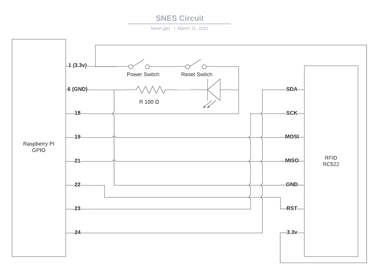
Here’s what I came up with:
A few immediate caveats:
- The diagram shows both the power and reset switches as being normally open - that is, they do not allow signal to flow through. In which case, the behavior would be off. What we ideally want is the power button to be normally open, but the reset button to by normally closed. If not, we can do some inverting of the signals to get what we want. But it does mean our diagram is inaccurate.
- It’s possible the LED on the SNES is 5v. If so, we can still use the power signal to drive it; we’ll just want to use a 5v signal to release a 3.3v output to the GPIO pin, or use a 3.3v signal to release a 5v output to the LED.
- Do we perhaps have to worry about current if we’re splitting stuff across multiple peripherals? This is where my complete and total ignorance really comes into play. Quick Googling suggests we want to keep total current below 50mA, and the RF reader peaks at 26mA, so I’m gonna guess we’re fine here.
Not a huge amount to do in the meantime until I’ve got a spare SNES here I can use for parts. Once that’s done, I’m eager to see if we can use the existing power and reset mechanical switches and see what we’re working with. From there, we should be able to determine what needs inversion, etc.